Scanning confocal Raman spectrometer with AFM option
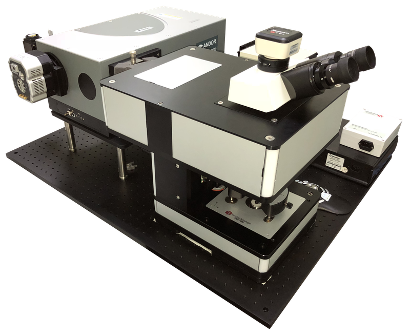 ARS3000
The main advantages of the system are:
- Compact size.
- Full automation of the system.
- The original design of the spectrometer.
- High light transmission of the device with minimal optical loss.
- The confocal circuit is made according to the original scheme, provides compact dimensions and minimal drifts of optical elements.
- Built-in optical microscope provides a convenient search for a place for measurements.
- The design uses precision mechanical components and optics.
- Can be used both in industrial laboratories and in research universities.
- Base configuration price 200 000 USD.
The main components of the system are: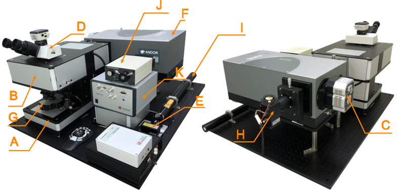
A. An automated base with a built-in flat scanner for the sample.
B. The confocal module containing the optical circuit of the excitation beam formation and the secondary (Raman radiation) detection channel.
C. Highly sensitive CCD sensor with deep cooling for recording secondary radiation spectra.
D. Trinocular optical microscope with the ability to observe the sample in both the eyepieces and the video camera.
E. Solid-state excitation laser, optional 355 nm, 473 nm, 532 nm, 785 nm. For connection of external lasers with other lines one-mode transport optical fiber is used.
F. Monochromator
G. Atomic Force Head for recording the signals of the sample topography.
H. PMU single-channel detector.
I. HeNe laser as a base for Raman spectroscopy.
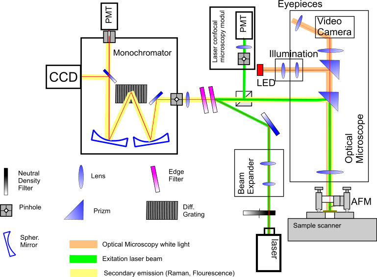
Optical scheme
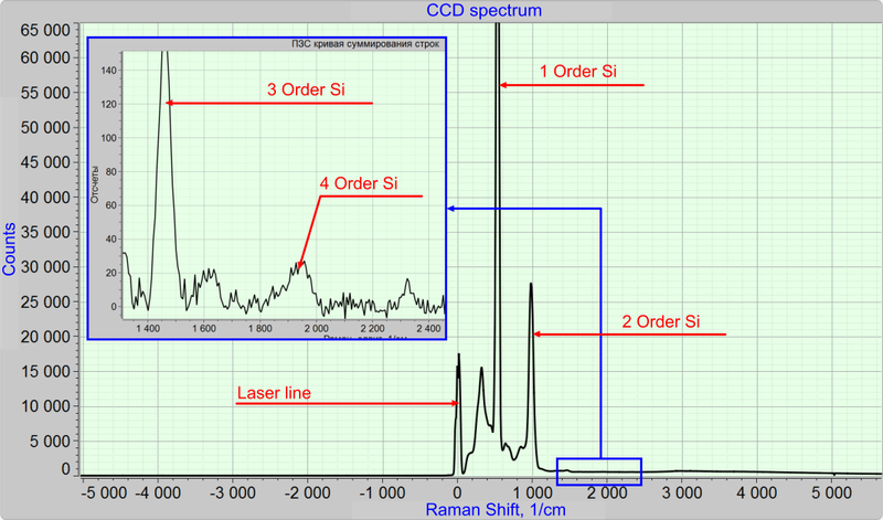
Optical sensitivity. 4 th order raman responce from silica.
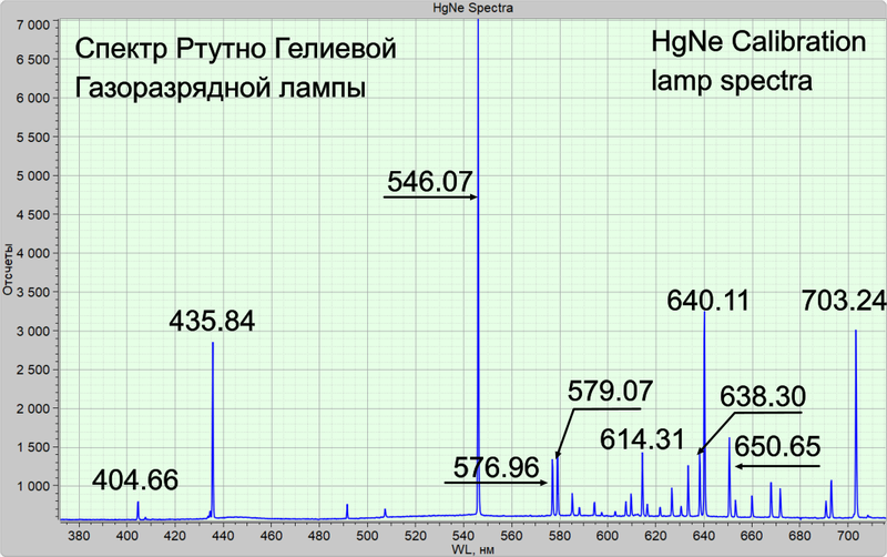
Spectral Resolution and range. HgNe calibration lamp spectra.
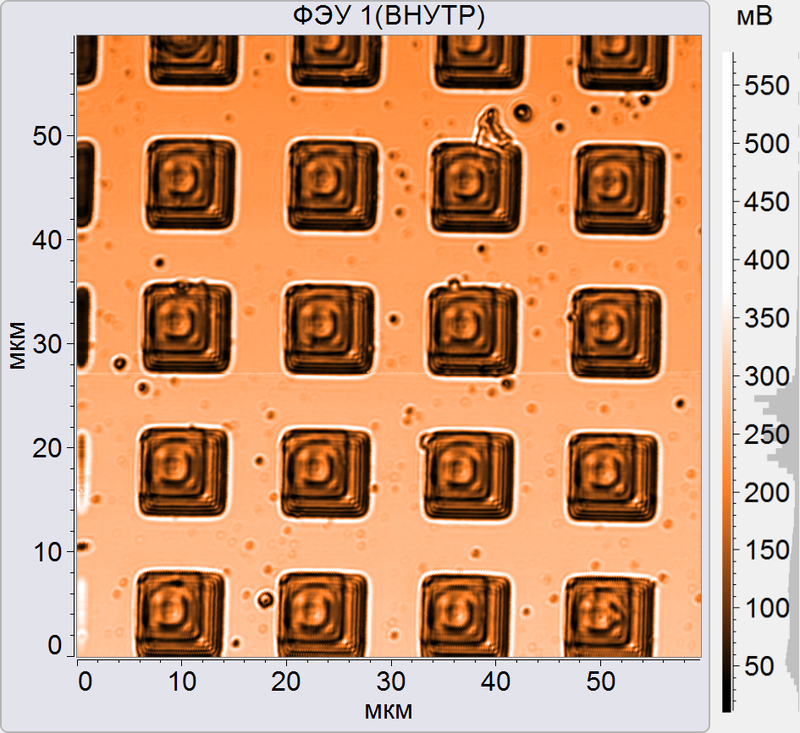
Surface optical maping:
 |
 |
|
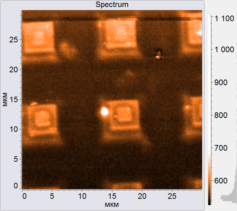
Laser confocal maping. Sample Si/SiO2 grating . |
Raman maping. Образец Si/SiO2 grating. |
 |
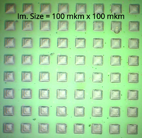 |
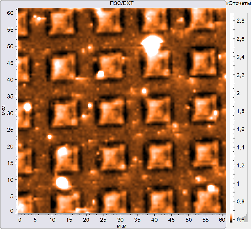
| Raman maping. Образец Si/SiO2 grating. | Optica Image. 100x magnification micro objective. |
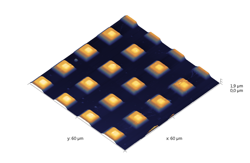
Atomic Force microscopy maping:
Base Specification:
| AFM resolution |
< 1 nm |
| Z AFM resolution |
<0.1 nm |
| Scanning range |
100x100x15 mkm |
| Secondary emission spectral range |
100..5000 cm-1 |
| Spectral resolution |
<1 cm-1 |
| Optical throughput |
>80% |
| Exitation laser |
532 nm |
| Detector Andor iVac 324 FI |
|
| Pixels number |
1560x200 pixels |
| Pixel size |
16 mkm |
| Cooling | till -60o |
| CCD read noise |
5.8 e |
| dark curent |
0.0028 e/pix/s |
| Мах speed |
269 spectra/s |
| Monochromator Andor Shamrock 500 i | |
| Focal distance |
500 mm |
| Diff. gratings |
|
| 150 lines/mm | Blaze WL = 500 nm, resolution = 0.52 nm |
| 600 lines/mm | Blaze WL = 500 nm, resolution = 0.13 nm |
| 1800 lines/mm | Blaze WL = 380 nm, resolution = 0.04 nm |
| Input pinhole |
Constant 100 mkm |
| Laser Cobolt |
|
| Type | NdYg |
| WL |
532.8 nm |
| Power | 25 мВт |
| Linght width |
< 1 pm |
| Upright optical microscope Olympus BX51 | |
| Illumination system |
Diod source |
| Power |
100W |
| Illumination Type |
Kohler |
| Eyepiece | widefield с 10х/24 mm |
| Interdistance |
50-70 mm |
| Trinocular with light path selector |
Prizm 0:100, 50:50 |
| Focus system |
Motorized |
| Accuracy |
100 nm |
| VideoCamera Moticam 2X |
|
| Type |
1/2” CMOS |
| Resolution, px | 2500x1800 |
| ADC resolution |
12 бит |
| Pixrl size |
2.5 мкм |
| Interface | WiFi |
| Microobjective module |
|
| Type | Turret for 4 objectives |
| Objective 1 | |
| SLMPLN 50X | |
| Optical amplification | 50x |
| N.A. | 0.35 |
| WD | 18 mm |
| Objective 2 |
|
| MPLFLN 100X | |
| Optical amplification | 100x |
| N.A. | 0.9 |
| WD | 1 mm |
| Sample positioning |
|
| Type | Motorized XYZ |
| Range | 10x10x10mm |
| Accuracy | 1mkm |
| AFM head positioning |
|
| Type | Motorized XY |
| Range | 10x10mm |
| Accuracy | 1mkm |
| Optical, AFM, scanning system |
|
| Тype | Flat XYZ stage |
| Range |
80μmx80μmx15 μm |
| Resolution |
< 0.01nm |
| Accuracy |
< 1nm |
| image nonlinearity |
<1% |
| Position sensors |
|
| Type |
Optical encoders with sin/cos interpolation, 300 kHz sampling rate, built-in autocallibration |
| AFM unit, AFM head Certus |
|
| PSD sensor | 4 sectioned PD |
| Laser spot arrangement | 2 micro screws with 0,125 mm pitch |
| PSD arrangement | 2 micro screws with 0,125 mm pitch |
| Tip scanning system is optional |


